![]()
![]()
My plans for conversion are fairly simple. Lets start off with an overview of the XV50 transverter. In receive mode, the essence of the operation is to amplify and mix the 50MHz with a 22 MHz local oscillator to produce a 28 MHz IF. On transmit, a 28 MHz signal is mixed with the 22 MHz LO to produce a 50 MHz signal which is then amplified to 20W. Conversion could involve simply replacing the 22 MHz LO with a 42 MHz LO which after a re-tune will in theory allow the transverter to operate at 70 MHz. None of the IF filtering and none of the RF switching circuitry needs to change.
The steps involved are:
While this may seem like a lot, it is not really all that much in practice, the areas where work is needed are shown in the figure. The most difficult is likely to be step 7. The remainder of this page explains what needs to be done. There is a procedure at the end if you wish to go ahead.
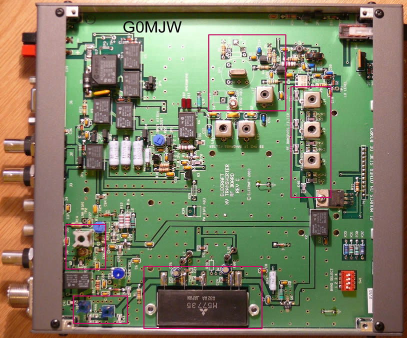
Crystal Oscillator
Lets start off with the crystal oscillator. The original XV50 uses a 22 MHz fundamental mode Colpitts oscillator. The simplest modification is to replace this with a 42 MHz crystal oscillator based on a 42MHz 3rd overtone series resonant crystal.
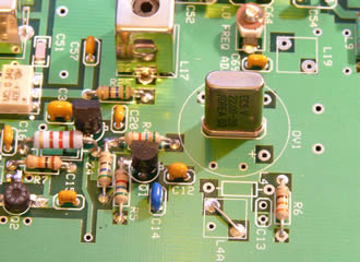
Here is an idea for the circuit:
The component numbers do not all relate to the XV50 parts because this is a different circuit. Rx and CX and LX are added. CX is simply DC blocking.
Here are the values:
Rx 560R, C12 56pF, C14 47pF, LX 7T on 1/4" close wound but ideally a trimmer if you want the lo to be exactly 42MHz, CX 100pF (Re use C12) . LX can be fitted in the vacant place of L19.
R4, R5, R6, Z4, C20, C15, Q1 and C33 are unchanged. Note that this is not the only option. If you are starting from an unpopulated PCB you can avoid cutting the track by using a circuit similar to that used in the XV144 with L4.
Filters
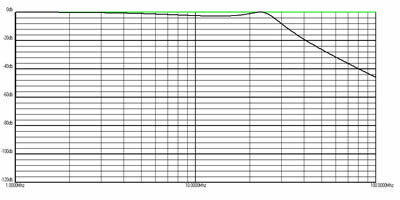
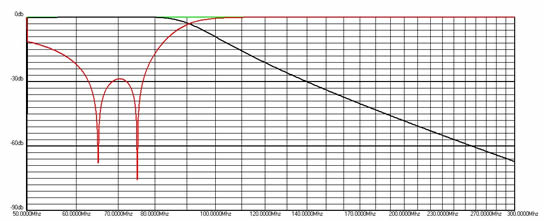
Following the crystal oscillator is a low pass Chebyshev filter made up from C58, C59 and L3. To operate at 42MHz, C58 and C59 need to be changed to 200pF and L3 to 120nH.
The figures show the predicted loss characteristics of the original and modified filter.
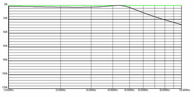
A more complex filter follows the mixer. This is a band pass design. Each component needs to be changed and that includes the coils which would be a lot of work.
Tuning the coils to minimum and just changing the capacitors is possible though less satisfactory in terms of the high frequency cut off, however, it is much easier and not so very bad as the plots show. The real problem is likely to be the image at 98 MHz (2x28 + 42) where this filter is only 35 dB down. Compare this with the original design where the worst image was at 72 MHz (28 + 2x 22) where the filter was down by 45 dB. The difference is not great, however, generally there is nothing at 72 MHz whereas 98MHz is in the broadcast band. In the plots below, note that this is with unoptimised inductors, the tweaking of the inductors will get rid of most of the ripple in the 50MHz response.
The new calculated values are: C48 and C51, 6.8 pF, C45 and C47 10pF, C46 15pF. The rest are unchanged but the coils are tuned close to minimum inductance. The scope for tweaking at 70MHz is limited because of the coils. It is best to start off with less shunt capacitance in each place and then add capacitance in parallel in the C45a, C46a and C47a positions if the coils can not peak the 70MHz band.
The final two filters are the transmitter low pass and the receiver pre-amplifier input.
The low pass output filter adjustment is a straight forward frequency scaling exercise. The original values of L10 and L11 I measured at 160nH, they are specified as 240nH coils but the slugs are removed. I used my own coils as I have a useful capacitance/inductance meter for this sort of task from AADE - whose filter analysis package produced the plots.
New Low Pass filter
If scaling, C42 and C43 are reduced to 56pF, C44 is reduced to 110pF and L10 and L11 are reduced to 115nH. As I did not have any 115nH coils and did not fancy winding some, in my transverter L10 and L11 are now both 100nH as I had some coils available and this simulates reasonably well. It is relatively easy to wind the coils on a T50-6 torroid if you prefer, it will only need a few turns of 1mm enameled wire. The new values for C42 and C43 are 60pF and for C44, 120pF. This works nicely. 120pF is a standard value. With series and parallel combinations it is possible to make up these values from series and parallel combinations of 120pF capacitors and also improve the power rating. Two in series gives 60pF and four in series/parallel gives 120pF at higher power.
The pre amplifier is matched by C28, C1 and L1. Frequency scaling of these components is non-trivial without the noise matching data for the FET Q3. As the circuit is fairly broadband in any case, a reduction of C28 to 10pF and of L1 to 0.24uH (I.e Recycle the replaced L11 as L1) puts the circuit in the right region. A worthwhile addition to this circuit, especially if you operate high power at 50MHz or live near a broadcast transmitter is a narrow band 70MHz pre-selecting filter.
Power Amplifier
The M57735 PA module does not really work well at 70MHz. If your XV50 uses the more recent MOSFET module, you can feel good about it. Otherwise, it is necessary to replace the bipolar module with a MOSFET module. The changes are not that bad and are entirely practicable with the existing PCB as it was designed to take either type of module.
This section goes into a lot of detail. If you know what you are doing, feel free to skip it and just follow the circuit diagram.
Collect together all the parts you need as outlined above and remove the top cover of your XV50. Admire it while arranging anti-static precautions. Note that the PCB uses plated through holes, these are tricky to unsolder, you need a hot iron, a good solder sucker and plenty of patience.
Preparation requires access to both sides of the PCB. This requires removal of the PA module, the M57735. This module does not work well on 70MHz and needs to be replaced, but there is no need to damage the module, it might come in useful some day.
Undo the bolts holding in the PA module. Remove the base cover from the transverter. Carefully de solder the PA module and remove it. Solder a 47 ohm resistor between the PA module input and ground - the ground pad of C24 is a good place. This resistor provides a load to the driver amplifier and will be removed when the PA module is replaced.
Crystal oscillator conversion
Unsolder the 22MHz crystal. This will not be reused. Remove C12, C14, C69 and C64. This is tricky but using a wire off cut to allow you to heat both pins at once helps. C14 and C69 are especially difficult as one side is grounded and heat sunk by the ground plane. The easiest thing to do it to cut it in half and take out each pin from the top individually. Capacitors are cheap. Replacing the new capacitors is not trivial as you will find it almost impossible to clear the holes of solder. Clear away as much solder as possible, cut the new capacitor leads to 5mm and insert the capacitor from the top of the pcb using solder and the iron on both pins at once. A gently push will get it through. Then move to the rear of the PCB, heat the leads again to melt the solder, push the capacitor fully home from the top side and tidy up the joints.
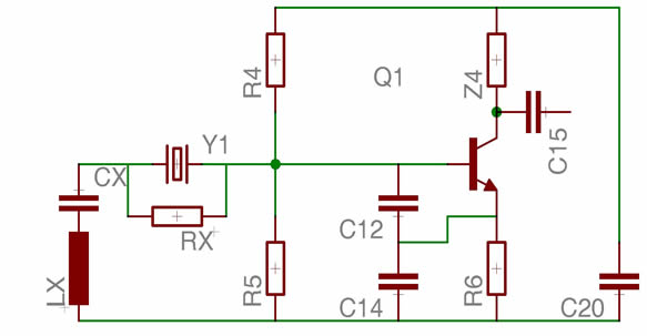
Carefully cut the track between C69a and C64. Then install a 100pF capacitor across the gap using the holes vacated by C64 and C69.
Install the new 42MHz crystal and fit a 560 ohm resistor in parallel on the underside of the PCB. Remove C58, C59 and L3 and replace with the new values. To make 200pF the simplest method is to use a 180pF capacitor in the holes and fit an 18pF capacitor in parallel under the PCB. L3 can be a purchased component, or you can wind it using the standard formula. I used 7 turns of SWG26 close spaced on a 1/8th inch former.
At this point, you could test the LO, however, you should make sure you only do this with the rest of the transverter disabled to reduce the chance of shorting things out - I.E pay attention to J9 pins 5&6 shorted and the power switch off. If you find you can not get the frequency exactly right, you may have to experiment with the value of LX. Remember, it you are using a K2 or K3 getting the frequency stable is more important than getting it exact as offsets can be corrected at the IF. The voltage measured at the LO test point should be around 0.8 to 1.2V.

New Resistor and cut track. Extra capacitor added as crystal was not getting onto frequency. I had not defluxed it at this stage, I have now.

This shows the LO from the top. Notice the new coil in place of L19, the unusual location of the capacitor by C69 and the new home made L3.
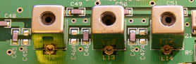
Mixer filter conversion.
The difficulty in removing the capacitors in the oscillator section should have convinced you why we will not change the coils in the filter. The modifications involve the removal of C45 to C51. These are all SMT components and the simplest and most effective removal method is to use two soldering irons. With C1 set to almost minimum it should now be possible to pick up noise and even signals on the 70MHz band. These can be used to peak the modified band pass filter if you have no other test gear. My unit at this stage had a conversion gain of 26 dB. The specification for the original XV50 transverter on 6m is 25 dB though I suspect this is conservative.
Low noise Receive Amplifier conversion
The low noise amplifier works fairly well as supplied on 70MHz simply by setting C1 to minimum. If you are using a mast head pre-amp it is probably good enough, however the sensitivity can be improved by changing L1 and C28. Now is the time to do this, remembering that FETs are particularly sensitive to static discharge damage.
Transmit Low Pass Filter
It is very important to modify the low pass filter as 70MHz is already significantly attenuated with the stock filter. L10 and L11 are now both 100nH as I had some 100nH coils available and this simulates reasonably well. The new values for C42 and C43 are 60pF and for C44, 120pF Remember that this part of the circuit operates at significant power - use appropriately rated low loss capacitors here. My replacement LPF is not too pretty as the coils were not an exact fit and the capacitors in series look odd. However, this filter produced a measured loss of under 0.2 dB at 70MHZ and had the predicted rejection of 30 dB at 140MHz and 60 dB at 210MHz.

The replacement LPF.
Transmit power amplifier
The transmit PA module must be replaced by one designed to work at 70MHz. There are a few choices here. The most obvious is to use the RA30H0608M now used by Elecraft. Using this module requires the circuit to be changed to match that of the XV144. DO NOT just replace the module, it will be destroyed.
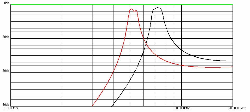
Before replacing the power amplifier module, it is worthwhile to simply bridge over the gap with a short length of coax. This will give you a QQRP signal on 70 MHz to test with. If you are using the XV70 to drive an amplifier, or another mixer, the power at this stage may already be sufficient. Here is the response I got at this stage. There are some spurious responses that I will investigate, but they remain at least 60 dB down until you over drive the mixer.
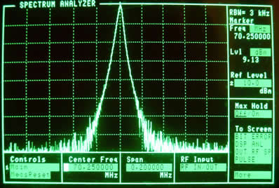

Close in and wider plots at just under 10mW output

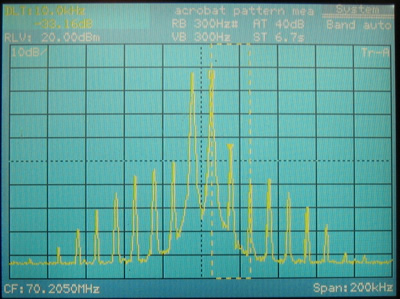
A plot at 50mW - Spurii starting to be a problem
Replacing the PA module is fairly simple. Remove the two jumpers in the bias circuit and replace with the same value components as used in the XV144. Remove the 5V link to the bias pin of the module and short jumper W. Remember to add the 1K resistor near to the module input. THen test you got it right before installing the module by measuring the voltage at the bias pin, it should be about 3-4V. Now follow the instructions in the manual for installing the PA module. Adjust the PA bias control so that the transverter takes around 0.8 to 1.5A on TX with no input power depending on if you wish to operate SSB or CW. Double check the heatsinking of the module, calibrate the power output meter. Then follow the remaining transmit section alignment instructions according to your drive configuration.
With the module replaced, a two tone test was attempted using two signal generators and a hybrid combiner. Input was -20 dBm from each generator with one set to 28.2 MHz and the other to 28.21 MHz. The levels of both tones were balanced to account for any gain variations in the filters. RF output was controlled using the IF gain pot. PSU voltage was 13.5V and PA module bias 300mA.
The IMD results are shown in the following table:
| XV70 IMD Tests | 10 W PEP Output | 20W PEP Output | 30W PEP Output |
| Each tone | 0 | 0 | 0 |
| 3rd order | -25 | -23 | -18 |
| 5th order | -34 | -34 | -29 |
| 7th order | -38 | -39 | -38 |
| 9th order | -43 | -44 | -42 |
| 11th order | -48 | -47 | -44 |
| 13th order | -54 | -51 | -47 |
| 15th order | -65 | -58 | -49 |
| 17th order | -70 | -65 | -50 |
| 19th order | Noise | -70 | -53 |
Note that the ARRL give results relative to total PEP. To get those figures, you need to subtract 6 dB from the above numbers. This result confirms that the transverter should really be operated below 10W SSB output if you wish to use less bais to keep it cool. The IMD can be improved by increasing the PA bias current but only at the expense of efficiency. Setting a high standing current is a problem as the module will still generate a lot of heat even without any RF output which the Elecraft case heatsinking method will have trouble dealing with. The improvement in IMD performance at higher bias is marked. The following table shows what happens with approximately 900mA of module bias current representing a standing dissipation of 12W, about the limit for cooling.
| XV70 IMD Tests | 10 W PEP Output | 20W PEP Output | 30W PEP Output |
| Each tone | 0 | 0 | 0 |
| 3rd order | -33 | -28 | -20 |
| 5th order | -47 | -39 | -37 |
| 7th order | -45 | -48 | -45 |
| 9th order | -51 | -49 | -55 |
| 11th order | -57 | -53 | -56 |
| 13th order | -64 | -58 | -54 |
| 15th order | Noise | -61 | -56 |
| 17th order | Noise | -65 | -59 |
| 19th order | Noise | -72 | -60 |
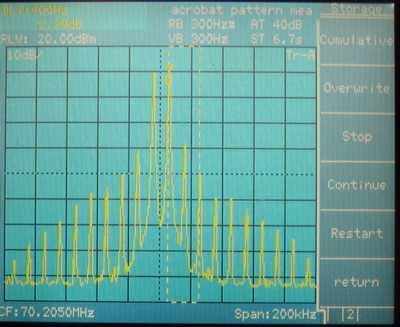
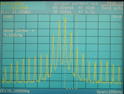
Here are some photos of the spectrum analyzer screen at 900mA module bias - Sorry about the quality, I didn't have it connected to the network to download them electronically. The response is not perfectly symmetrical though both tones are at the same level.
10W Output
20W Output
30W Output
I hope these instructions help someone, but note I can't take any responsibility for any unforeseen problems etc. that might arise from them.
Copyright G0MJW 2008